
FPGA IP Cores and Partnerships
")

We are DSP FPGA, DSP Programming, SDR Radio Software, Packet Processing, and Algorithm experts.
Get to market quickly by utilizing Apogee’s advanced FPGA IP Cores, or let Apogee investigate implementing your specific algorithm in an FPGA:
100 GbE FPGA IP Core Description – 2024 Q3
10 GbE FPGA IP Core Description
Multi-Channel High-Speed Real-to Complex Core
Multi-channel CIC filter Core w/Roll-off Compensation and Variable Output BW Filter
100 Gigabit Ethernet Core
The 100Gb Ethernet processing core will support client side connections to AXI4 Streaming RX and TX interfaces. The core will directly connect to the AMD/Xilinx CMAC IP hardcore in the Ultrascale+ FPGAs. The core is controlled during run time by an 32-bit AXILite memory mapped interface.
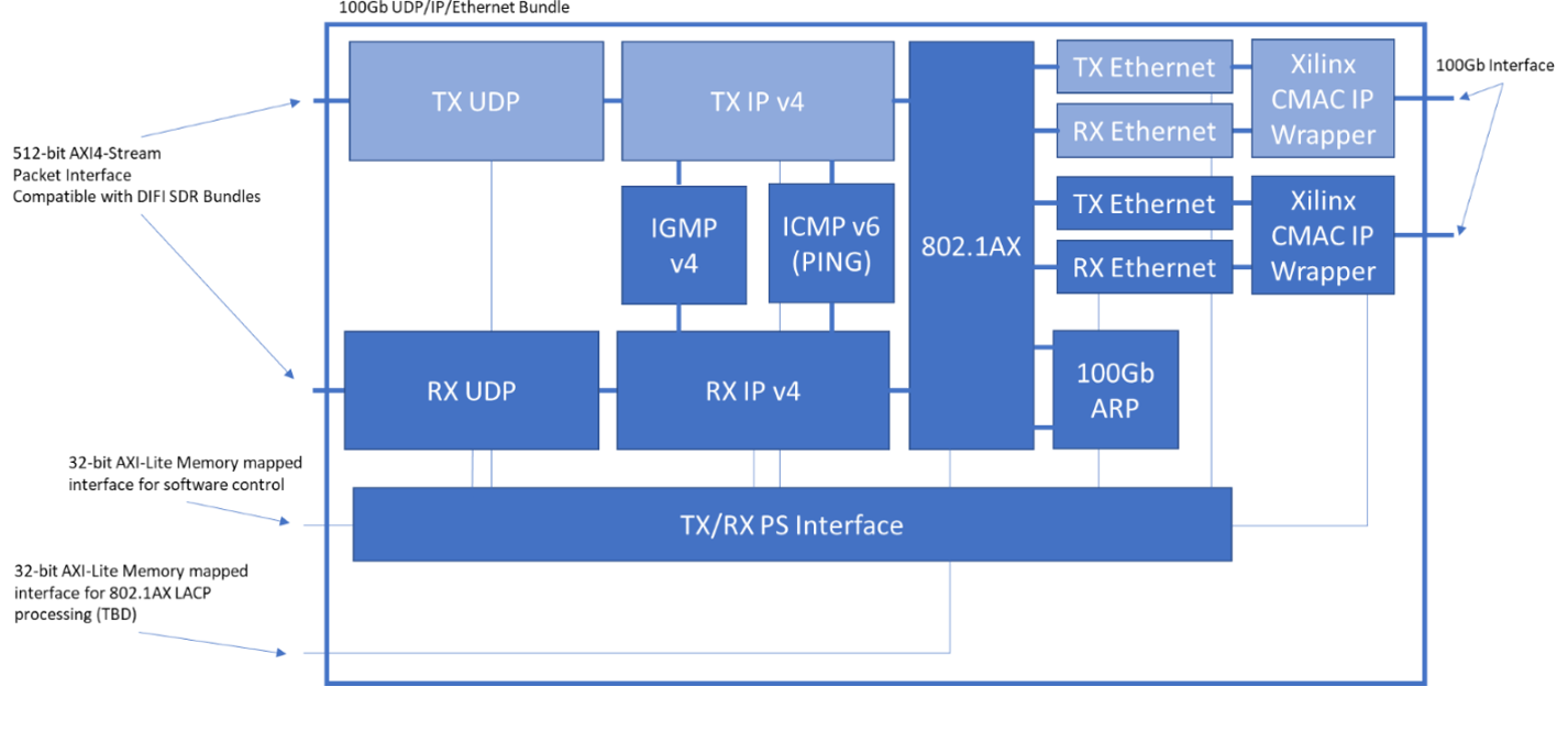
100 Gb Ethernet packet processing core supporting:
- UDP RFC 768
- IPv4 RFC 791
- including header checksum calculations and verification
- excluding fragmented packet generation and reassembly
- IEEE 802.3 Ethernet
- VLAN 802.1Q and VLAN 802.1ad (QinQ)
- IGMPv2
- Scalable multi-channel
- Pseudo-Random timers for report generation
- ICMP v6
- Ping/Echo support only
- Interfacing to AMD/Xilinx Ultrascale+ CMAC core
The core supports buffering for 9000-byte Jumbo frame MTU size. The core can still receive larger MTUs but will drop the frames.
10 Gigabit Ethernet Core (1 Gigabit Core also available)
The Ethernet processor handles the break-down and analysis of incoming packets and the generation of outgoing packets. It handles the Physical (10GbSFP+), Link (Ethernet, ARP), Internet (IPv4, IGMP), and Transport (UDP) layers (TCP/IP also available). The Ethernet processor uses a dual proprietary micro-coded Finite State Machine(FSM) to process the incoming and outgoing packets. The FSMs are connected for the handling of automated response packets such as ARP and IGMP. Each FSM contains a large 512 entry table for storage and high-speed search of the possible packet addresses. The address table contains the MAC address, VLAN, IP, and UDP port. The processor supports multicast using IPv4 and IGMPv2 and IGMPv3. 10 GbEIP Core Data Sheet
SDR Packet Processor Core
The SDR Application Layer Packet Processor processes incoming and outgoing Software Defined-Radio FPGA packets. The App Processor utilizes Apogee’s Finite State Machine (ApoFSM) packet processor to quickly process 512-channels of inbound and outbound packet headers. The processor operates on the application layer (Internet Protocol Suite Model) of the packet. It currently supports formats such as SDDS and is architected to support VITA49. The processor is designed to interface with the aurora modules.
With the incoming packets, the processor handles interpreting and removing the packet header, storing timecode and frequency information in local memory, and presenting the packet payload and format information to downstream processing. On the transmit side, the outgoing packets are received as formatted payloads with a timecode offset value and sideband formatting information. The App Processor then calculates the new timecode based on the received sample offset and timecode memory address values.
There are also two modules, an unformatter and formatter that are used to break the data into samples and put samples back into a payload format. The unformatter receives the packet payload and sideband formatting information. The information is then used to break the payload into data samples that are then sent downstream. The sideband information contains minimum information to unpack the data. The formatter does just the opposite in formatting the data samples into a packet payload. The unformatter and formatter are separate modules that can be instantiated or left out depending on the requirements of the processing.
Multi-Channel High-Speed Real-to-Complex Core
The Real-to-Complex Core converts up to 64-channels of real signal data into complex baseband signals, all the while maintaining 80% bandwidths. The input is 4 samples wide to support up to 4 times the processing clock frequency. The inputs also support complex data at up to 2x the rate for selectable pass through. The inputs are 16-bit twos-complement. Each sample maintains a channel number to delineate between different streams. There are no restrictions on the order of channels coming into the core. The inputs are gated with a input valid signal so the input data can be at any sample rate less than or equal to than 4 times the processing clock.
Multi-channel CIC filter Core w/ Roll-off Compensation and Variable Output BW Filter
The Cascaded integrator-comb (CIC) filter is an efficient implementation of a decimating filter. The filter has dual independent inputs, each with 32-channels. The inputs support individual channel sample rates up to Fclk/6, and aggregate sample rates up to 2 times the processing clock frequency. The input handles 16-bit, twos-complement data. The CIC filter roll-off is compensated internally.
The output bandwidth can be selected, on a per-channel basis, in 5% increments from 5% to 80%, which allows for a significant reduction in filter requirements in downstream processing such as arbitrary resamplers in rate tracking loops.
Packet Switch Core
The Packet Switching core routes packets from sources to destinations. Each source and destination handles up to 512-channels. Packet sizes can be between 1 and 1500 Bytes (Inquire about larger sizes). The packet switches handles fanout to multiple destination ports but not multiple channels on the same port. It currently supports 1100MB/s transfer rates per port. The switch contains minimal buffering reduce the logic requirements. The packets are routed based on the source port and a 9-bit channel field in a 64-bit header on each packet. Packets are routed using a channel number, there is no PHY, High-Level IP, or MAC address switching.
Interpolating Resampler
- Single Channel, performs a variable fractional rate interpolation on the input signal
- Output rate is always module clock rate
- Interpolation range from 1.5625 to 200; 2^-17 phase step
- 32-bit control word (fractional interval). U_ctrl = (fsin/fclk)*2^31 (fractional interval)
- Modified Farrow Architecture (16 polynomials that are 5th order)
- Filter characteristic scales with rate change
- 16-bit complex input 18-bit complex output
- Capable of running in excess of 300 MHz in Xilinx V6-2
- DSP48E1=106, FFs=2919, LUTs=4079
- Stock filter shape ensures 70 dB dynamic range, for specific requirements filter shape can be modified

